Join TMAX, become an agent!
Join TMAX, become an agent!
Sales Manager: Gia
Email: Gia@tmaxlaboratory.com
Wechat: Dingqiuna
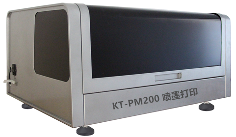
Item No.:
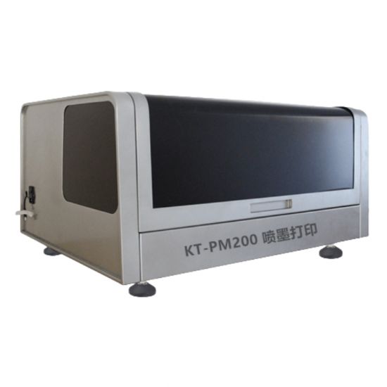
TMAX-KT-PM200Certificate:
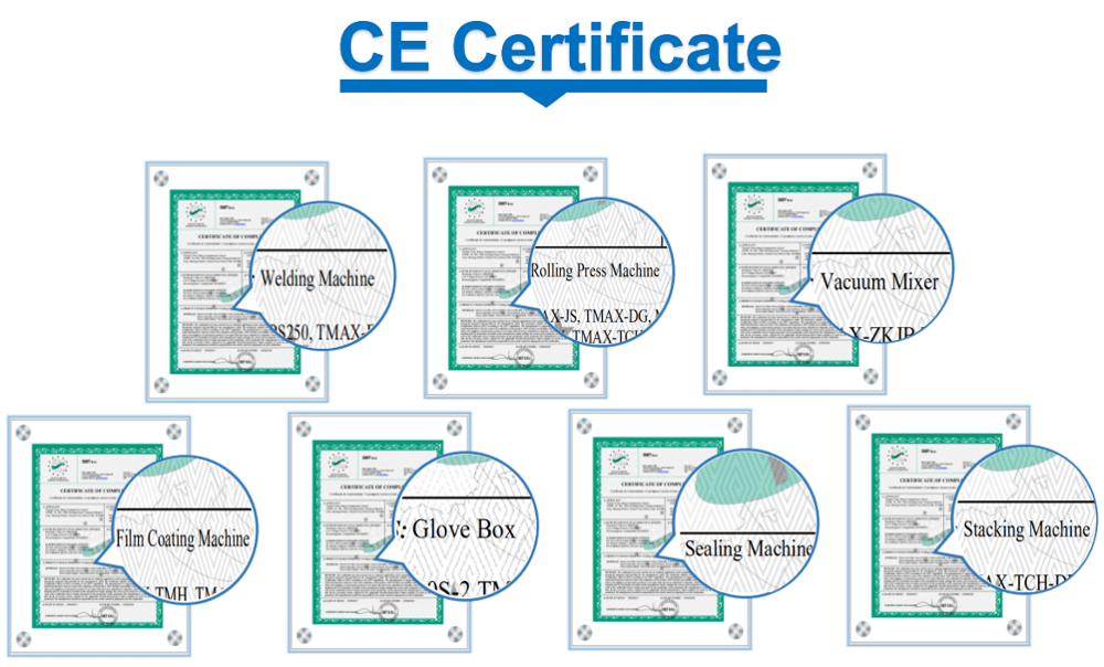
CE CertifiedWarranty:
1 Year limited warranty with lifetime supportMiniature 2400dpi High-Precision Printing Inkjet Printer Used for Perovskite Solar Cell Lab Line
A. Product introduction:
Inkjet printer has been applied in the field of perovskite solar cells due to its features such as high material utilization rate, low cost, high process efficiency, patternability, and large-area fabrication. In the preparation methods of perovskite solar cells, the small-area perovskite solar cells fabricated based on inkjet printing technology have achieved an efficiency close to 20%, with the highest reaching 22.7%. While the perovskite solar cells manufactured by traditional solution spin coating method have an average efficiency of around 16% and the highest efficiency is 19.4%. Therefore, the inkjet printing technology for manufacturing perovskite solar cells has gained popularity in terms of conversion efficiency. Inkjet printing also has advantages such as high uniformity of the formed film and good film formation properties. It can be applied to materials in various directions, including solvents, water-based, and UV. The application fields include printed electronics, flexible electronics, organic electronics and bioelectronics, etc. It can be used for printing and manufacturing various microelectronic circuits, RF antennas, 5G antennas, sensors, electric heating electrodes, etc., and can also print test OLED ink, TFE ink and quantum dot ink, etc. for touch screens and OLED/QLED lighting display fields.
B. Product features:
a.Piezoelectric waveform: Open waveform control software
b.The edge trimming and thinning function balances the ink diffusion
c.Negative pressure adsorption and heating platform
d.Single nozzle with dual channels, with 192 spray holes in each channel
e.The printing platform adsorbs and heats the substrate
f.The minimum printing line width and line spacing are 50-75 μ m
g.The single-print thickness range of the material is 20-200nm (adjustable freely).
h.Support graphic pixel pre-trimming edges
i.It can be combined with near-infrared nanophotonics sintering
j.It can be equipped with heating for the inner channel of the nozzle
k.Independent 4 nozzles
l.Visual CCD alignment and registration
m.Multi-material parallel and serial printing
n.3pl small ink dots, open waveform
o.2400dpi high-precision printing
p.UV curing module
C. Technical specifications:
|
Parameters |
Indicator |
|
Motion axis |
Three axes, X,Y,Z |
|
Printing platform |
Negative pressure adsorption, heated |
|
Print size: X*Y |
297mm*210mm |
|
Print height Z |
0~10mm |
|
Mechanical repeatability accuracy |
0.02 mm |
|
Number of nozzles |
Standard configuration: 2 (supports 4) |
|
Ink droplet size |
Minimum 3.0pl |
|
Ink type |
Compatible with water-based, solvent and UV ink |
|
Printing accuracy |
0.075mm to 0.1mm |
|
Ink supply principle |
Four independent negative pressure ink supply systems |
|
Ink stack module |
Four sets of independent ink stacks, moisturizing |
|
Supported format |
1-bit TIF, DXF,Gerber *, 3D slice files stl, 3mf, 3ds, etc. (*DXF,Gerber formats are provided with RIP software) |
|
Resolution |
1200*1200, 2400*2400 |
|
Curing lamp |
365nm UV curing lamp |
|
Power supply/power |
220V/50Hz, 1.5kw |
|
External dimensions |
960mm(L)x709mm(W)x618mm(H) |
|
Equipment working environment |
Temperature: +20℃ to +30℃ Relative humidity: 40% to 60% |
|
Application |
Preparation of electrode circuits, OLeds, solar cells, sensors, semiconductors and other devices |
|
Optoelectronic device preparation |
Including perovskite, graphene, carbon nanotubes, OLED/QLED, OPV, OTFT, quantum dot ink, sensors, TFE packaging, PI printing film, bank inkjet printing, etc. |


Previous :
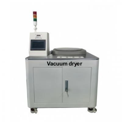
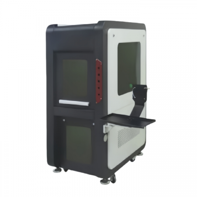
355nm Wavelength Vertical Type Laser Marking Equipment with Ultraviolet LaserNext :
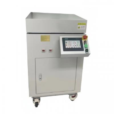
Lab 100mm or 150mm Film Width Automatic Scraping Coating Instrument for Perovskite FilmsCategories
Sales Manager: Gia Email: Gia@tmaxlaboratory.com Wechat: Dingqiuna
Sales Manager: Gia Email: Gia@tmaxlaboratory.com Wechat: Dingqiuna
Sales Manager: Gia Email: Gia@tmaxlaboratory.com Wechat: Dingqiuna
Sales Manager: Gia Email: Gia@tmaxlaboratory.com Wechat: Dingqiuna
Sales Manager: Gia Email: Gia@tmaxlaboratory.com Wechat: Dingqiuna
Sales Manager: Gia Email: Gia@tmaxlaboratory.com Wechat: Dingqiuna
Sales Manager: Gia Email: Gia@tmaxlaboratory.com Wechat: Dingqiuna
Sales Manager: Gia Email: Gia@tmaxlaboratory.com Wechat: Dingqiuna
For inquiries about our products or pricelist, please leave to us and we will be in touch within 24 hours.
© Copyright: 2026 Xiamen Tmax Battery Equipments Limited All Rights Reserved.

IPv6 network supported