Join TMAX, become an agent!
Join TMAX, become an agent!
Sales Manager: Gia
Email: Gia@tmaxlaboratory.com
Wechat: Dingqiuna
Item No.:
TMAX-SD-02Payment:
L/C, T/T, Western Union, Credit Cards, PaypalShipping port:
Xiamen PortLead Time:
5 DaysCertificate:
CE, IOS, ROHS, SGS, UL CertificateWarranty:
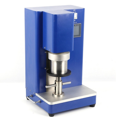
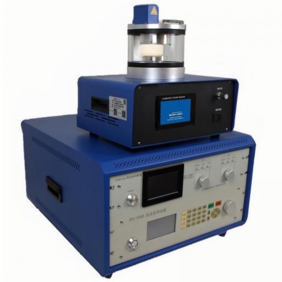
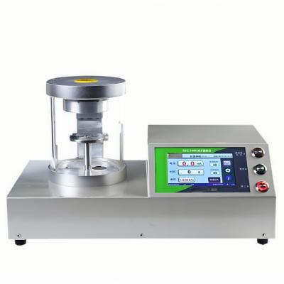
Two years limited warranty with lifetime technical supportPVD Magnetron Sputtering System for Thin Film Deposition – Ideal for Research Labs, Semiconductor Prototyping, and Optical Coating
Model: TMAX-SD-JS02-Sputtering System for Research Labs, Semiconductor Prototyping, and Optical Coating
Product Overview
The Plasma Magnetron Sputtering System (Model: TMAX-SD-JS02) is a compact, user-friendly instrument designed for high-quality thin film deposition. With a quartz chamber (150 × 120 mm) and a maximum sputtering rate of 8 nm/min, it is ideal for research and small-scale production requiring precise, uniform coatings. Compatible with inert gases (Ar, N₂) and versatile metal targets (Au, Ag, Pt, etc.), this system combines efficiency with advanced operational features.
|
Parameter |
Specification |
|
Quartz Chamber Size |
150 × 120 mm |
|
Sample Stage Size |
70 mm (diameter) |
|
Sputtering Area |
50 mm (diameter) |
|
Max. Vacuum Degree |
5 Pa |
|
Process Gases |
Argon, Nitrogen (flow rate adjustable) |
|
Max. Sputtering Rate |
8 nm/min |
|
Power Consumption |
200 W |
|
Dimensions (W×D×H) |
360 × 310 × 150 mm |
|
Operating Temperature |
0–40°C |
|
Relative Humidity |
< 85% |
|
Installation |
Horizontal desktop placement |
1. Intuitive Control & Monitoring
4.3" color touchscreen with graphical interface for real-time display of sputtering current, voltage, and vacuum levels.
2. Flexible Gas & Target Options
Adjustable inert gas flow (Ar/N₂) and support for 50 mm diameter metal targets (1–2 mm thickness), enabling quick material swaps and process reproducibility.
3. Modular & User-Centric Design
·Split-type quartz chamber for easy maintenance.
·Height-adjustable sample stage (±20 mm) with rotational alignment.
·Auto-venting post-sputtering simplifies sample handling.
4. Compact & Reliable
·Space-saving footprint with multi-layered software protections for extended durability.
5. Uniform Film Quality
·Dense, homogeneous coatings compatible with noble and transition metals (Au, Ag, Pt, etc.).
· Research Labs: Thin film studies, surface engineering, and material science.
· Semiconductor Prototyping: Deposition of conductive/metallic layers.
· Optics & Electronics: Functional coatings for sensors or display components.
Note: Optimized for small substrates (≤50 mm) and low-to-medium throughput requirements.


1 Standard exported package: Internal anticollision protection, external export wooden box packaging.
2 Shipping by express, by air, by sea according to customers' requirements to find the most suitable way.
3 Responsible for the damage during the shipping process, will change the damage part for you for free.

Previous :
SEM Low-Temperature Mini Magnetron Sputtering System EquipmentNext :
RF Magnetron Sputtering System for Metals & Non-Metals: Insulators, Semiconductors, Carbon-Based Thin Film DepositionCategories
Sales Manager: Gia Email: Gia@tmaxlaboratory.com Wechat: Dingqiuna
Sales Manager: Gia Email: Gia@tmaxlaboratory.com Wechat: Dingqiuna
Sales Manager: Gia Email: Gia@tmaxlaboratory.com Wechat: Dingqiuna
Sales Manager: Gia Email: Gia@tmaxlaboratory.com Wechat: Dingqiuna
Sales Manager: Gia Email: Gia@tmaxlaboratory.com Wechat: Dingqiuna
Sales Manager: Gia Email: Gia@tmaxlaboratory.com Wechat: Dingqiuna
Sales Manager: Gia Email: Gia@tmaxlaboratory.com Wechat: Dingqiuna
Sales Manager: Gia Email: Gia@tmaxlaboratory.com Wechat: Dingqiuna
For inquiries about our products or pricelist, please leave to us and we will be in touch within 24 hours.
© Copyright: 2026 Xiamen Tmax Battery Equipments Limited All Rights Reserved.

IPv6 network supported