Xiamen Tmax Battery Equipments Limited was set up as a manufacturer in 1995, dealing with Laboratory equipments, technology, etc. We have total manufacturing facilities of around 2, 000 square meters and more than 100 staff. Owning a group of experie-nced engineers and staffs, we can bring you not only reliable products and technology, but also excellent services and real value you will expect and enjoy.
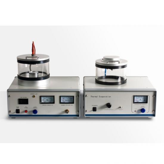
PVD Sputtering Coating: Advanced Thin-Film Deposition Equipment for High-Performance Surfaces
Overview
PVD Sputtering Coating technology represents one of the most advanced and widely adopted methods for depositing thin films with high precision and excellent performance. A PVD sputtering coating system is a vacuum-based machine that utilizes plasma-assisted sputtering to transfer atoms from a solid target to a substrate surface, forming a dense and uniform coating. Compared with traditional coating technologies, PVD sputtering coating equipment offers superior control over film thickness, composition, and microstructure. As a result, it has become an essential solution in modern manufacturing and scientific research fields such as electronics, optics, tooling, energy, and surface engineering.
Key Features
Modern PVD sputtering coating systems are designed with high mechanical stability and intelligent process control to ensure consistent coating quality. A high-vacuum chamber is a core component, typically supported by multi-stage pumping systems that achieve low base pressures and minimize contamination.
These systems commonly support multiple sputtering modes, including DC sputtering, RF sputtering, and magnetron sputtering, enabling the deposition of both conductive and non-conductive materials. Advanced power supplies and mass flow controllers allow precise regulation of sputtering power, working pressure, and gas composition. User-friendly interfaces, often based on PLC or touchscreen control, enable real-time monitoring and repeatable process recipes. Optional configurations such as multi-target carousels, substrate rotation, heating, and biasing further enhance coating uniformity and functional performance.
Sputtering Process and Working Principle
The PVD sputtering coating process begins with loading substrates into the vacuum chamber and evacuating it to the required base pressure. An inert gas, most commonly argon, is then introduced into the chamber. When electrical power is applied to the target, the argon gas becomes ionized, forming a stable plasma.
Positively charged argon ions are accelerated toward the negatively biased target surface, where their kinetic energy causes atoms to be physically ejected from the target. These sputtered atoms travel through the vacuum and condense onto the substrate, forming a thin and adherent coating. In reactive sputtering processes, reactive gases such as nitrogen or oxygen are introduced to form compound coatings like nitrides or oxides. By precisely controlling process parameters, PVD sputtering coating systems can produce films with thicknesses ranging from a few nanometers to several micrometers.
Sputtering Machine
Applications
PVD Sputtering Coating equipment is widely used across a variety of industries. In the semiconductor and microelectronics sectors, it is essential for depositing conductive layers, diffusion barriers, and functional films on wafers and electronic components. In optics, PVD sputtering coating systems are used to produce reflective, anti-reflective, and interference coatings on lenses, displays, and optical components.
In the tooling and automotive industries, sputtered coatings enhance wear resistance, hardness, and corrosion protection of cutting tools and mechanical parts. The technology is also critical in energy applications, including thin-film solar cells, battery electrodes, and fuel cell components. Additionally, PVD sputtering coating systems are extensively used in research institutions for advanced materials development and surface modification.
Advantages
One of the main advantages of PVD sputtering coating is the ability to produce dense, uniform, and highly adherent films with excellent mechanical and functional properties. The process operates at relatively low substrate temperatures, making it suitable for temperature-sensitive materials.
Another key benefit is material versatility. A wide range of metals, alloys, oxides, and nitrides can be deposited using the same system. The coating process is clean, environmentally friendly, and highly repeatable, supporting both laboratory research and large-scale industrial production. Furthermore, precise control over film thickness and composition ensures consistent quality and high performance.
Conclusion
In conclusion, PVD Sputtering Coating systems are indispensable thin-film deposition machines in modern industry and research. With their advanced features, precise process control, and broad application range, they provide reliable solutions for producing high-performance coatings that meet the demanding requirements of today’s advanced technologies.